
Demystifying the semiconductor process node
Its more complicated that you think it is

Disclaimer: Opinions shared in this, and all my posts are mine, and mine alone. They do not reflect the views of my employer(s), and are not investment advice.
When companies like Intel, Apple, or Nvidia release a new chip, one of the first metric that is mentioned is the chip node - for example, the A18 Bionic chip in the iPhone 16 was build on TSMC’s 3nm process node. Being the first chip on the latest node is a bragging point for processor makers. I had a very basic understanding of what a node means from my undergraduate semiconductor classes, but my recent research revealed that there is a lot more to this magic number.
The good old days (1970 - 1995):
In 1960s, after the invention of the transistor, the goal of chip makers was simple - try to pack more transistors within a given area. To quantify how good the process of making such a chip was, the semiconductor process node was defined as the minimum feature size in the manufacturing process - basically, what is the smallest dimension that can be present in your chip. As it turned out, the smallest dimension usually was the length of the transistor’s gate - so that was chosen to represent the node. For example, the transistors used in Intel 4004 were 10 μm in length. Hence, the process node was called the 10 μm node.
This is a diagram of an nMOS MOSFET transistor, with the gate length highlighted:
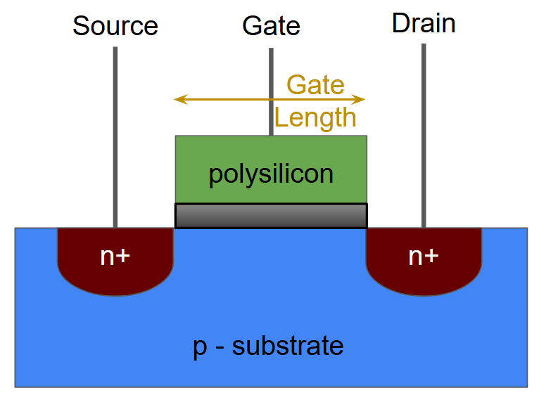
If you think of a transistor like a switch, the gate is like the bridge the connects the two ends. Typically, when a transistor’s gate is made smaller, the following happens:
The supply voltage needed to operate the transistor can be reduced.
Taking the bridge analogy further - if the bridge is smaller, electrons need lesser “force” to move from one side to another. If the supply voltage is lower, the power consumed each time a transistor switches is also going to be lower, so the chip overall will consume lower power per transistor.
The transistor switching is faster
Again, smaller bridge means lesser time to cross the bridge. This means changing state between 0 and 1 is faster, which means the chip can be run at higher frequency.
Smaller gate = Smaller Transistor
Which means more transistors can be placed in the same area.
Given all these advantages, there is a clear benefit to make your chip with a smaller process node. As a result, till around 1990s, semiconductor manufacturers worked to reduce the gate size in each generation, and the node was defined based on this new gate size. Remember, the transistor scaling was driven by Moore’s law (Here is a link to my post about it) - so the goal was to roughly double the transistor density. This means reducing the area occupied by each transistor to half. Typically, when the gate size is scaled, the overall length and width of the transistor could also be scaled. So by scaling the gate size to 70% of the current size in each generation, the transistor density could be doubled. This is roughly seen in Intel’s roadmap during the 1970s - 1990s.
10 μm (10,000 nm) - 1971
6 μm (6,000 nm) - mid-1970s
3 μm (3,000 nm) - late 1970s
1.5 μm (1,500 nm) - 1982
1 μm (1,000 nm) - mid-1980s
0.8 μm (800 nm) - late 1980s
0.6 μm (600 nm) - early 1990s
0.35 μm (350 nm) - 1995
It is after the 350 nm node, when things started to get interesting…
The end of symmetric scaling (1997 - 2010):
In 1997, Intel was set to release the 250 nm node - but the transistor gate length was 200 nm. So why was the new node called 250 nm and not 200 nm? Intel, and other companies that followed, realized that by this point in the industry, the semiconductor node strongly corelated with the number of transistors that could be packed in a chip. The processors at this time had more than a million transistors, so the individual transistor size started to matter less. Although the gate was reduced to 200 nm, other dimensions of the transistor did not scale at the same rate. So they started to look at the area occupied by a bigger cell - like an SRAM.
Intel’s 350nm process (P854) had an SRAM cell area of 18.1 µm². In the first version of their 250 nm node (P856), the SRAM cell area dropped to 10.26 µm², and in the improved version that came out next year (P856.5), the SRAM cell area was 9.26 µm². So an SRAM cell built with the 250 nm has roughly half the area of one build with the 350 nm node. So if the 250 nm node also had a symmetrical transistor (all dimensions scaling together) like the 350 nm node, the equivalent gate length would be 350 nm * 0.7 = 250 nm.
This same trend continued till 2012, with SRAM area improving by 40-50% to justify the naming of the new node. This is the list of Intel’s process nodes from 250 nm to 32 nm, with the SRAM cell area and approximate gate length.
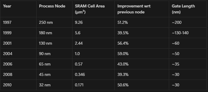
Notice that the cadence of new node being released was consistently around 2-3 years, and the process node is always very close to 0.7 times the previous node - this shows clearly the shift from node being an actual dimension to just a abstracted marketing number.
The era of FinFETs and TSMC (2012 - 2024):
If you notice in the table above, through the 65, 45, and 32 nm nodes, the gate length remains roughly the same. Transistor gate size had gotten so small, that further shrinking led to a phenomenon called quantum tunneling - which would make the transistor switching unpredictable. To avoid quantum tunneling, the channel in the transistor was raised to cut through the gate like a shark's Fin, resulting in a new type of Transistor called FinFET. The Fin increased the surface area of the channel and allowed more electrons to pass through - providing the same effect that reducing the gate size would. This is a figure of a FinFET from a post by Semiengineering that highlights the fins.
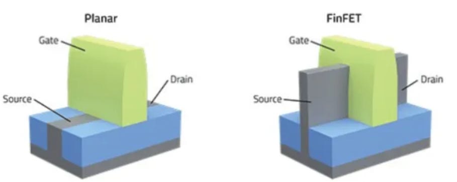
Unlike traditional transistors, where the length and width of the transistor were the only scaling factors, FinFETs added a third factor - the channel height. (This is why FinFET is called a 3D transistor). Also around this time, the goal of Moore’s law was shifting more toward “how to get better performance within some area/power constraint”. Hence, simply looking at dimensions of a transistor did not give any idea about what the resulting chip could do.
This time period also saw the emergence and dominance of TSMC, who shifted the focus away from transistors. This was a major shift in the industry. You can think of earlier chips like handwritten manuscripts - and the evolution of transistors was like moving from quilts to fountain pens. However, TSMC realized that the way forward was not better ink, instead it was a better printer! Along with the support of equipment manufacturers like ASML, TSMC pioneered the use of many innovations in VLSI process, like EUV and Multi-Patterning, to make new nodes better. For example, to shift from the N14 to N10 node, TSMC was only able to make the standard cell size in N10 83% that of N14. However, they improved the process (using triple patterning) to reduce the overall chip area to 56%, which gave an overall improvement of 47% from N14 to N10.
In addition to the change in transistor and fabrication technology, the working model of coming up with a new node has also changed significantly. Earlier, designers and fabs worked independently, and designers made their design assuming that transistor density would double (or follow whatever Moore's law's definition was at the time). But now, a closer relationship started to develop between the two groups - this process is called Design Technology Co-Optimization (DTCO). This was needed because as the nodes got smaller, the design rules got more complicated, and the stakeholders needed to work together to make these new nodes possible. There was also a business reason - DTCO introduced a new variable along with Performance (P), Power (P), and Area (A) - Cost of the wafer (C). The goal of these discussions is to come up with a process that meets the PPAC requirements of the chip design company. As a result of DTCO, every node is unique now - For their recent 3 nm node, TSMC has multiple variations - N3, N3E, N3P, N3X, N3S (and also some private nodes for major customers) - each of these promise a different PPAC. IMEC has proposed a new model called System Technology Co-optimization - STCO - which would add more variables into deciding on a semiconductor process node.
Essentially, the semiconductor manufacturing industry has become so complicated now, that summarizing everything using a single number is impossible. I have heard this argument made a lot, even by very established people in the industry - “10A is less than the size of an atom, it will be impossible to have a node so small, Moore’s law is dead”. I’m sure we will have nodes smaller that the size of an atom. The reason is that the semiconductor node has become a mere marketing term today. While in general, smaller nodes are better, we cannot draw a clear comparison between nodes anymore, especially with different foundries. For example, Intel's 10 nm density is better than Samsung's 10 nm, and comparable to TSMC's 7 nm. So a lot of these processors announcements that only highlight a better node will need to be taken with a grain of salt.
References:
wikichip.org - a great resource for information about different semiconductor process nodes.
Techquickie - Should You Believe CPU Marketing? - Process Nodes Explained
Anastasi In Tech - What is wrong with 5nm, 3nm, 1nm.. CPU Technology Nodes explained