


Power essentials for a chip architect
All you need to know about power as a chip designer

Disclaimer: Opinions shared in this, and all my posts are mine, and mine alone. They do not reflect the views of my employer(s), and are not investment advice.
Before going ahead, let me define what I mean by some terms from the title of this post:
Chip: I’m talking specifically about computing chips like a CPU or GPU
Chip Architect: Someone who works on architecture or microarchitecture of a chip
Power: Energy consumed by a chip from a battery or a electrical socket per unit time.
Essentials: Only what an architect needs to know - everything else will be abstracted out
When a CPU or GPU is designed, there are three key metrics: Performance, Power and Area. (commonly combined in the acronym “PPA”.) Of the three, I have always found power to be the least intuitive. In most textbooks and college courses, power consumption is explained through the physics of the transistor. (i.e. movement of electrons.) While it’s good to know these details, I have always felt that not knowing them shouldn’t stop you from thinking about power. (In the same way that a web designer needn’t know all the details of the cloud in which their website is hosted.)
So, that’s the goal of this post: to go over essential concepts needed to design a low power chip if you are someone who knows a good amount about chip architecture, but very little about power.
Let’s get started.
Part 1: Fundamental ideas in power
When does a chip consume power: The rental car analogy
Before looking at the impact of design decisions on power, it’s important to understand the two ways in which power is consumed in a chip. To make this simple, consider this analogy: Chip power is like the money you spend on a rental car each day.
Let me explain further. Imagine that you are on a trip and have rented a car. The amount of money you would spend on this car daily can be divided into two components:
Daily rental charges (depends on the type of car, rental company, and so on)
Fuel expenses per day (depends on your usage of the car)
Chip power also has two similar components:
Static power: Power that is consumed anytime the chip is on
Dynamic power: Power that is consumed to perform some logic in the chip
As you may have figured, static power is like the daily rental charges you pay: As long as the chip is turned on, even if there is no new task to be run, power is still consumed. On the other hand, dynamic power, like the fuel cost, depends on the number, and type of logic operations that a chip executes.
Why do these two types of power matter?
Usually, when you rent a car, all you care about is the total amount of money you spend. So you might be wondering why we want to split up the power consumption into two different types. The reason why we do this, is because power alone is not a useful metric. There are two metrics that derived from static and dynamic power which are actually important:
Energy consumed
As you know, power is energy per unit time. So the energy consumed by a chip would depend on the amount of time for which static or dynamic power is consumed, in addition to the values themselves. In our rental car analogy, you can think of energy consumed as the total money spent on the rental car during your trip - which includes rental charges for each day of the trip, and fuel expenses incurred every time you drive the car. At a very high level, this is what you need to know:
Static power is consumed for the full duration when the chip is connected to a power source
Dynamic power is consumed only when the chip is actively executing a task
Energy consumed by a chip is an important metric, because:
In battery operated devices, lower energy consumption means a longer battery life without needing to recharge
In plugged devices (connected to an external power source), lower energy consumption means a smaller amount on your electricity bill
If the goal is to reduce the amount of energy consumed, one type of power could be more important than the other. There are two scenarios you may experience:
Scenario 1: When static power is more important
To understand this, let’s take the rental car analogy further. Imagine that your trip is designed in a way that for most of the days of the rental, you will not be driving the car. In this scenario, the daily rental charge is going to be more significant compared to your fuel expense. Like your rental car, a lot of chips today are designed for use-cases with high idle time.
A real-life example of this use case is a personal assistant device like Google Nest or Amazon Echo. Although these devices are plugged into a power source all the time, they spend majority of this time in an idle state. However, static power is still consumed in this idle state, making it the main contributor towards the energy consumption. Ideally, a chip designed for this use case should prioritize reducing its static power.
Scenario 2: When dynamic power is more important
This is the classic case of a road trip - where you spend most days actually driving your rental car, and in the process spending a lot on the fuel. In real circuits, dynamic power tends to be higher than static power - so although static power is still consumed here, reducing dynamic power becomes the priority. (Ideally, you would reduce both, but as you will see later in the post, there are tradeoffs involved in these design decisions.)
Many datacenters today are designed to maximize utilization of all the available compute all the time - at a chip level, a new task continually needs to be executed. In power terms, this means that dynamic power is being consumed (along with static power) during most of the time when the power supply is connected. Designing a chip that reduces dynamic power consumption becomes valuable in this scenario.
Peak Power
While power is usually correlated with energy consumption, (sometimes, the two are incorrectly interchanged) there is another metric that is actually more important - Peak Power, which is the maximum power consumed at any point during which the chip is on. In other words, it is the power when the sum of static and dynamic power is the highest. Imagine being told that you have a daily allowance for the money you spend on your rental car (including fuel expenses) that you are not allowed to exceed - that’s what Peak Power is.
There is a reason why I said Peak Power is more important than energy consumed - while higher energy consumption would result in smaller battery life or a bigger electricity bill (which are bad, but don’t make the device unusable.), Peak Power directly impacts the operation of the chip. If the peak power is high, a few things can go wrong:
Too much heat is produced
Unexpected voltage drops occur
Complex power distribution network are needed
Each of this could be catastrophic, as Nvidia once learnt the hard way. During the design on their NV30 chip in 2002, Nvidia were forced to increase the clock frequency of their chips in order to be competitive with ATI’s Radeon 9700 PRO. But without realizing it, this exceeded their Peak Power budget, and resulted in excessive heating. In what was a last minute move, they added a huge dual-slot fan to ensure that the chip was still usable. But this fan was very loud, and as a result, NV30 became the butt of many “hot chip” jokes. (In fact, Nvidia posted a spoof video themselves.)
Peak power is a very interesting topic in itself, with challenges in both estimation, and management techniques. But for the purposes of this post, the main takeaway is this: while there could be many design decisions that are effective at reducing energy consumption, they are only valid if they are under the peak power budget.
So far, we’ve understood that there are two types of power consumed in a chip - static and dynamic power. Changes in these two types have power has consequences on two important metric in chip design - Energy consumed and Peak power. Trust me, this is all you need to know about power as a chip architect. Once you are equipped with this knowledge, the next step is to look at some techniques that architects follow to reduce power consumption.
Part 2: Power optimization
If you have read this post so far, you know the basic concepts in chip power, and are ready to put your “low-power chip architect hat” on. When I was reviewing this topic, I found a lot of solutions proposed were either constrained to a very specific design, or were slightly different versions of the same idea. (often wrapped around fancy terminology.) In order to keep this section simple and clear, I’m proposing a new hierarchy for ideas. For both static and dynamic timing, we will classify ideas as:
Principles: the fundamental ideas that can apply to any design
Techniques: a specific implementation of a principle
Techniques are huge in number, and can be implemented at both the architecture, and microarchitecture levels. I’ll share few example techniques of each type for each principle, but I urge the reader to focus more on the principles. Note that whether a technique is good or bad depends on how it impacts other key metrics in the chip - which includes area, performance, peak power, and energy consumption. Since these requirements vary based on the end-application for the chip - there is no one good technique.
With these logistics out of the way, let’s start with static power.
Static Power Optimization
As we saw earlier, static power is always consumed when a chip is kept on. A nuance that I want to add here is: each transistor consumes static power independently. This leads us to the two principles to reduce static power consumption.
Principle 1: Reduce Transistor Count
If we go back to our rental car analogy, and consider each transistor as a rental car - then it becomes clear that your daily rental charge increases for each additional rental car you have. So the most obvious way to reduce static power is to reduce the number of transistors in your chip. Since this post is meant for a chip architect, transistor count reduction is same as area reduction by removing or simplifying big logic blocks in the chip. Here are some such techniques:
Technique 1: Remove Redundancy
Let me use an example to explain the idea of redundancy. Consider executing a CPU instruction to do the following:
Read data from register 1
Read data from register 2
Add them
Store the result in register 3
We read/write register data using a block called register file. The number of parallel reads that can be executed by the register file is decided by the number of register ports. This means:
If we have 2 read ports, data from register 0 and 1 can be read in the same cycle
If we have 1 read port, we read data from register 0 in the first cycle, and data from register 1 in the next cycle.
It should be clear that 2 read ports result in better performance than 1 read port. But an additional read port costs additional area, which means more transistors, and higher static power.
In theory, you only need one instance of each type of block in a chip - one adder, one register/memory port, and so on. But redundancy is a common attribute in most chips that is used to improve performance. If reducing static power is your main goal, removing such redundancy can help. Typically, this also reduces the peak power of the chip. However, energy consumption could vary from case to case - it is possible that reducing redundancy results in a huge performance penalty, and as a result, you need to run the chip for longer and consume more energy to do that. Hence, a good understanding of the application is key before making a decision to reduce redundancy.
Technique 2: Eliminate Pipelines
If you are unaware of what a pipeline is, I recommend one of my earlier posts on CPU pipelines. Each pipeline stage added comes with an area cost - which means additional transistors consuming static power. So by combining different pipeline stage together and reducing the number of pipeline stages, static power can be reduced. (This also reduces dynamic power, but we will look at that later.)
However, pipelining is a common technique to increase the frequency, and hence throughput of the chip. So by removing pipelines, you may save on area, peak power, and even energy consumption in most cases - but it comes at the cost of a significant performance drop.
Technique 3: Simplify Prediction
If you look into any modern computing chip, you will find different “hacks” that are meant to improve execution performance. I’ve put them under a bucket called “prediction” - as these methods build on knowing something about the data or instruction patterns. Two common methods in this bucket are:
Branch/Value prediction
Caching
Although these result in a performance bump, to get better prediction results, you would need more complex hardware blocks. (As an example, you can check the different cache mapping schemes I discussed in an earlier post.) Complex blocks means more transistors, and more static power. By simplifying these techniques (For example, using a direct mapped cache instead of a set associative cache) we can reduce static power consumption.
Much like reducing redundancy, estimating how this technique would reduce energy is tricky: Recovering from cache misses may result in additional energy consumption - and this may overshadow the reduction from static power savings.
Principle 2: Reduce Transistor Voltage
If you have a large group and cannot reduce the number of cars you are renting, the next best option would be to find a rental company that gives you the best deal. In circuit land, this “deal” actually comes from the voltage applied on the transistor. In layman terms: the transistor is like a resistance - when you apply a higher voltage, more current flows, and this increases the static power. To reduce static power through reduced voltage, apply these coupon codes at your rental car checkout:
Technique 1: Power Gating
What's the best way to reduce the voltage applied to transistors in a chip? How about not applying any voltage? Well, you can’t do that for the whole chip, because that would just make it a block of silicon. That's where power gating comes in - instead of turning off the entire chip, only the unused parts of a chip can be turned off. Since static power is only consumed by the transistors that are connected to a voltage source, power gating effectively reduces the number of active transistors - which reduces the static power consumed.
Power gating is done in real time - which means, as a chip architect, designing the chip in a way that would allow larger blocks to remain off for a longer time, while still maintaining the similar performance, becomes the key. It is also important that there is some way to detect if, and when a certain block would be unused. The complex logic needed to handle power gating introduces some area overhead - still, power gating is one of the most commonly used techniques to reduce static power.
Technique 2: Multi-Voltage Islands
This is another similar idea to power gating - but instead of turning off the voltage for some blocks in real time, a lower voltage is used. Low voltage is different from no voltage, because with low voltage, the logic is still functioning - it is just slower. (I'm skipping the details, but transistors running on lower voltages can only support lower frequencies - this is what makes the chip slower.) So as an architect, you could divide the entire chip into different voltage domains (i.e. logic blocks sharing a voltage source) based on the expected usage, and reduce the voltage for the domains that can run slower. Another way to use the same idea is to use the same chip design to support different applications by changing the voltage applied to each domain.
Irrespective of the implementation, using multiple voltage domains (or islands) is an effective way to lower static power for some parts of the chip (and hence lower the total static power.) If done correctly, this may also not have a major performance impact, although it would increase the chip area.
Technique 3: Dynamic Voltage Scaling
As I mentioned in the previous technique, reducing transistor voltage is possible if the frequency is also reduced. This is the idea that Dynamic Voltage Scaling (DVS) exploits. With DVS, the circuit has the ability to lower the voltage applied (and simultaneously reduce frequency) when slower execution is acceptable - imagine an application that has a burst of heavy processing that happens at once, followed by periods of light processing. The static power can be reduced by lowering the voltage when heavy processing is not needed.
As an architect, identifying opportunities for DVS, and building in the capability to detect DVS is key - and often comes with an associated area cost. In most cases, it would also lead to lower performance. But it is commonly used in battery operated devices - when you are running low on battery and hit the “power saving mode” on your smartphone - it’s DVS at work. DVS also impacts dynamic power, which I will cover in the next section.
Dynamic Power Optimization
If you remember our rental car analogy, I mentioned that dynamic power is like the fuel expense incurred each day on your car. When I was first learning to drive a car, I came across many different theories on how to reduce your fuel consumption - from simple concepts like “accelerate/brake gradually”, and “use cruise control on freeways”, to more obscure ideas like “For this car model, maintain tire pressure to be X, drive at speed Y, and have a candid conversation with your engine every Sunday” (I’m kidding of course… or am I?)
My point is, dynamic power is also similar - there are a lot of ideas proposed, with most being too specific to certain microarchitectural implementation or workload - which ultimately results in a lot of confusion. To avoid this, I’m going to try to use the same two tier hierarchy I proposed for static power, and hopefully rid you of some of the confusion.
Principle 1: Reduce active clock cycles
After driving for a few years, here’s what I learnt - if you want to reduce fuel consumption, just turn the engine off. In chip language, this means turning off the clock. (If you want to know about clocks and pipelines, check this post before reading further.) Here are some techniques to reduce active clock cycles.
Technique 1: Clock Gating
This is one of the most popular techniques to reduce chip power. Much like power gating, the goal is to identify blocks that are unused for some period of time, and turn their clocks off. Clock gating inserts logic (called the "gate") into the clock path going to a some related logic - this gate can be selectively turned on or off in real time. (typically based on some other logic in the chip.)
There are many nuances involved in implementing clock gating that I’m skipping in this post. But as a chip architect, identifying opportunities for clock gating is invaluable. A block is ideally suited for clock gating if:
It can remain off (the technical term is “idle”) for a significant time while the chip is still running
There is a way (ideally an easy way) to identify when the clock for this block needs to be active
Clock gating is a great way to save a lot of energy. (i.e. provide better battery life for your devices) In fact, in most cases, clock gating can be implemented with minimal impact on performance. (There are some cases, especially high frequency designs, where meeting timing with clock gating could be challenging, so take this with a grain of salt.) However, there would be some additional area cost - for both the control, and gating logic.
I want to end this section by talking about the interdependence between power gating and clock gating. It should be obvious that if power gating is implemented, then clock gating becomes redundant. However, power gating is usually more complicated, and incurs a bigger performance penalty - so in many cases, a hierarchical approach is followed:
If a block is idle, turn off the clock first (i.e. clock gating) - save dynamic power
If the block remains idle for very long, pull the plug (literally, i.e. power gating) - save both static and dynamic power
Technique 2: Dynamic Frequency Scaling (DFS)
When I talked about Dynamic Voltage Scaling (DVS) under static power optimization, I mentioned that it comes at the cost of reduced clock frequency. Taken independently, this frequency reduction comes under a technique known as Dynamic Frequency Scaling (DFS). Reducing the frequency means fewer clock cycles are completed in a second, which translates to lower dynamic power. However, when you are reducing the frequency, you are reducing the performance of the chip. But a clever usage of DFS can hide the performance drop from the user of the chip - for example, if your computer is turned on, but you aren’t actively doing something, (like playing a game, or watching a movie) there is no need for the highest performance. Detecting such opportunities is the challenge, and can be done broadly in two ways:
Through the operating system (this is called CPU throttling)
Through some hardware signals (for example, architects can add counters to indicate low usage)
Both methods would cost more transistors to implement, but the energy savings are worth the investment. Although you can lower the frequency without lowering the voltage, DFS and DVS are typically used together to get maximum power savings. This is called Dynamic Voltage and Frequency Scaling, or DVFS.
Technique 3: Efficiency Cores
When I first heard about a multi-core CPU, I expected multiple copies of the same core used to execute more than one task simultaneously. But power optimization was built into multi-core when in 2011, ARM introduced their “big.LITTLE” architecture. The idea was to pair high performance (”big”) cores with power-efficient (”LITTLE”) cores to get the best of both worlds. A dynamic task scheduler assigns the appropriate tasks to each type of core, ideally without any slowness that a user can perceive.
This idea has now been adopted by most multi-core CPUs, and is known generally as Performance-Efficiency (PE) architecture. While the Efficiency cores (E-cores) can use any of the power optimization techniques discussed in this post, I have placed this technique here, as the biggest power savings come from the lower clock frequency used by the E-cores.
Although in general, a Performance core has better performance than an Efficiency core, the smaller size of efficiency cores can allow more cores to be packed in the same area - so it is hard to convincingly talk about the performance impact of the multi-core system. Overall, the PE architecture has been quite revolutionary, and can be expected to remain a mainstay for the foreseeable future.
Principle 2: Reduce switching
I hope you aren’t tired of the rental car analogy already, but here I go, one last time. You can think of each switching event like a stop you are making while driving. A stop-start car ride is not going to be fuel efficient - similarly, more switching activity in a chip means more dynamic power. Unlike the previous principle, switching is heavily dependent on the workload and the microarchitecture. To make things easier, I have classified the sources of switching into two categories:
Switching in combinational logic (Think: Stops caused by vehicle traffic)
Switching in sequential logic (Think: Traffic lights, Stop signs, and so on)
I will provide some example techniques for each category, but you will see these are quite “hacky” and won’t be applicable more generally. Let’s start with combinational logic.
Principle 2.1: Reduce switching in combinational logic
This part of my post assumes some digital design knowledge, but if you don’t know what combinational logic is, here’s a layman definition: Any logic that does not use a clock is combinational logic. Some examples are Binary logic gates (like AND, OR, NOT), adders, comparators, and so on. Each time the voltage triggers combinational logic, dynamic power is consumed. Here are some techniques to reduce the triggers.
Technique 1: Remove Redundancy
I also mentioned this under static power optimization. In the context of dynamic power, if you have fewer blocks of a type, (say one multiplier instead of two) it also means that fewer blocks end up consuming dynamic power. An effective way to use this technique in a chip is by identifying logic that can be shared: For example, if you are using two different multipliers to multiply values from the same signal in different parts of the design, why not share the logic? But even an ideal candidate like this may result in routing issues. (what if the two parts of the design are very far away from each other in the final chip layout?) Hence, although peak power and area would be lower, this typically comes with a performance drop, and potentially consume more energy overall to recover from the lost performance.
Technique 2: Moving Logic Downstream
This title could be vague - so let me jump directly to an example.
Consider three values - A, B and C. Your chip needs to do this:
If A is greater than B, multiply A and C.
Else, multiply B and C
There are two ways to do this:
Option 1
Multiply A and C
Multiply B and C
Then compare the two products - the greater one is your final result
Option 2
Compare A and B - the greater one is your initial result
Multiply the result from the previous step with C
It’s obvious that Option 2 is better than Option 1 when it comes to dynamic power. In Option 2, we are doing multiplication in the last stage - as a result, we only need to do the multiplication once. In other words, to reduce dynamic power, move complex logic downstream, so you can limit the number of triggers to this logic.
This was a very simplistic example to demonstrate this technique - you might wonder why anyone would even implement Option 1 - because even the performance would be better in Option 2. While it is obvious in simple designs, but in large designs, such minor details often get missed - imagine the values A, B and C coming from completely different modules, passing through different pipe stages, or maybe even being handled by different teams! That’s what makes even simple techniques like this challenging to implement.
Technique 3: Digital Logic Tricks
If you have been working on digital logic long enough, some tricks become evident to you. For example, when I first started writing RTL logic, I used multiplications everywhere - just like you would in a software programming language like Python. But there are a lot of scenarios, where true multiplication is not necessary.
For example, Let’s say you want to multiply the values A and B - but you know B is always a power of 2. (i.e. 1, 2, 4, 8 and so on.) Then, instead of multiplication, this logic can be implemented using bit shifts. For example, If A = 5, B = 4, then A*B is same as 5 << 2. (i.e. shift the binary value of A to the left by 2 places.) In hardware, a shift logic is just wires, which means zero dynamic power - a far more power efficient implementation than using multipliers.
Another common trick related to multiplication is to bypass multiplication when you can detect one of the operands to be 0 or 1. We can skip multiplication here too, but remember that detecting 0s or 1s comes with an area overhead. (and may also increase the peak power slightly, to implement the extra logic.) But if the energy saved is significant, it is still worth doing.
There are many other tricks like this which a good designer has at their disposal to reduce combinational logic (and consequently the resulting dynamic power)
Principle 2.2: Reduce switching in sequential logic
Sequential logic refers to the structures that use clock and can maintain their state between clock cycles - the fundamental components are usually a flip-flop or a latch, which can be combined together to create bigger structures like registers, and finite state machines. (FSMs) Dynamic power is consumed by sequential logic during a clock event. (this typically happens when the clock signal moves from low voltage to high - called the positive clock edge.) This means that all the techniques under principle 1 will also reduce dynamic power consumed by sequential logic. However, this principle focuses on how to reduce switching by keeping the same clock frequency - in other words, how to switch fewer sequential logic elements in a chip.
Technique 1: Eliminate Pipelines
This was already covered under static power, and the same text applies here. Fewer pipeline stages means fewer flop stages, and as a result, lower dynamic power is dissipated.
Technique 2: Replace Registers with SRAMs
I mentioned that sequential logic is used to maintain state - this means they can be used as memory elements to store some data (bits) during the chip execution. The most common way to store data is using registers - which is a collection of 1-bit storage elements like flip-flops or latches. Each time a bit needs to be modified, these elements consume dynamic power - hence, large registers become a hotspot (pun intended) for power consumption in a chip.
Registers are not the only storage - Static Random Access Memories (SRAMs) are an alternative structure that can be used to store data. While the fundamental unit of an SRAM is similar to a register, they are packed together to serve as dense memories. (read as: area reduction.) But SRAM design has gone beyond just area density today. SRAMs are now designed with techniques like sleep modes, voltage scaling, and read/write gating to make them highly power efficient. (Also, in terms of logistics in chip teams, chip architects typically don’t design SRAMs - so as an architect, if you have a low power SRAM solution available from a different team or vendor, this becomes a plug-and-play power optimization technique for you.)
It’s important to note that simply replacing any register with an SRAM will not work - typically, the power benefits of SRAM are significant only for large memories. Also, if you are storing data once, but reading it often, then registers are actually better. (since they only consume dynamic power during the storage phase.) Also, SRAM access is slower than registers, which is likely to have an impact on overall performance. So use this technique cautiously.
Technique 3: Using pointers to avoid toggling
This is a very specific implementation, but I find it to be elegant, so it has earned it’s place here. (Good interview question too, by the way.) Let’s say you want to implement a First-In-First-Out (FIFO) structure, that can hold 4 elements. Here’s a simple way to implement this structure (called a shift register):
Place 4 registers (R1, R2, R3, R4) back-to-back, with the output of R1 connected to the input of R2, and so on
When a new entry should be added, send it as input to R1, and shift all existing elements one place (So the data held between R1 and R2, now moves between R2 and R3)
Once full, if you want to read the first (oldest) data, simply read the output of R4
However, the problem with this implementation is that each time a new entry is added, all 4 registers switch. Now imagine the same structure for 1000 entries, with each entry being 1024 bit wide - that’s a lot of dynamic power for each new entry.
A better (power optimal) way to implement the same design, is to have independent registers, along with pointers for each register. In the above example, if we had 4 independent registers, we could track the start, end and next pointer each time a new entry get added:
First entry - add it to R1, then set:
start pointer = R1
end pointer = R1
New entry added - add it to any available register (let’s say R3). Then set
start pointer = R1
end pointer = R3
R1’s next pointer = R3
Similarly, store new entries in any registers, and update start, end and next pointers accordingly.
If you notice, in this implementation, each time a new entry gets added, only one register needs to be updated. (ignoring pointer management, which would have a small area, power, and performance overhead.) This design could easily scale to large FIFOs without a big dynamic power increase.
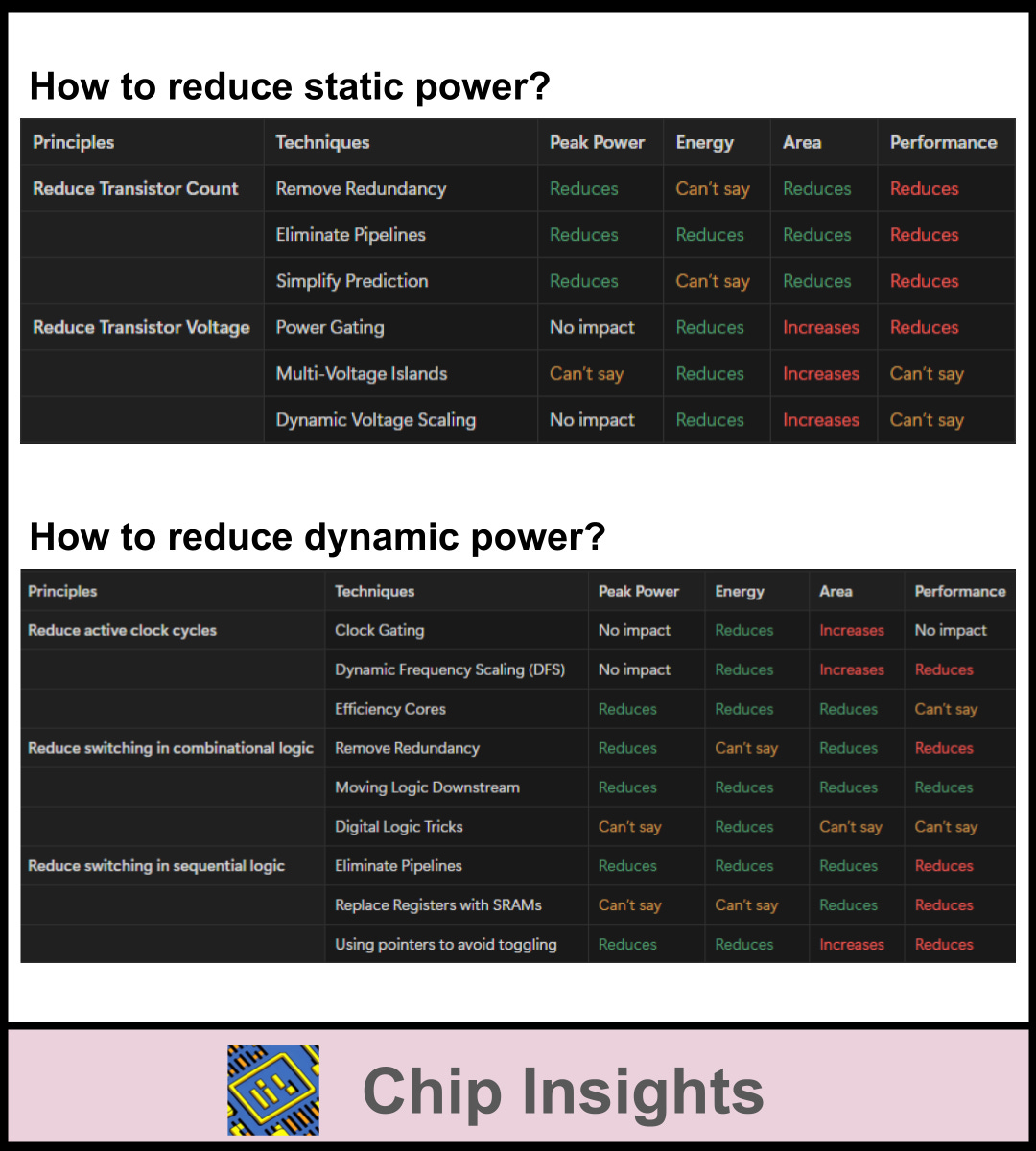
If you have read so far, here’s something to leave with: a table summarizing the principles and techniques discussed above, and their impacts on metrics. Remember that some metrics depend strongly on the workload being accessed - the results in the table only provides the general trend.
I want to reiterate something I mentioned earlier - this list of techniques in this post (and I’d argue any post) is not exhaustive - they are merely examples to understand the principles better. I hope you can take some of these ideas to build some incredibly power efficient chips in the future. Or at the very least, pass along your learnings - one way to do that is to share this post with someone you know :)
More power to you
A great analogy to explain static, dynamic and peak power